
Your shopping cart is empty! Please select the type which you want.
Printed circuit board(PCB)Wiring plays a key role in high-speed circuits,But it is often one of the last few steps in the circuit design process。high speedPCBThere are many problems with wiring,A lot of literature has been written on this topic.。This paper mainly discusses the wiring problem of high-speed circuits from the perspective of practice.。The main purpose is to help new users design high-speed circuitsPCBPay attention to a variety of different issues that need to be considered during wiring。Another purpose is to have not been in contact for some time.PCBWiring customers provide a review material。Due to limited layout,This article cannot discuss all the issues in detail,But we will discuss improving circuit performance、Reduce design time、The key part of saving modification time with maximum effectiveness。
Although mainly for circuits related to high speed operational amplifiers,但Yes这里所讨论of问题with方法对用于大多数其它高速模拟电路的wiring是普遍适用的。When the op amp is operating at very high RF(RF)Band time,The performance of the circuit depends largely onPCB布线。“drawing”High-performance circuit design that looks good on,If it is affected by carelessness during wiring,In the end, only ordinary performance can be obtained.。Pre-considering and paying attention to important details throughout the wiring process will help ensure expected circuit performance。
Schematic
Although good schematics do not guarantee good wiring,But good wiring starts with a good schematic。Be thoughtful when drawing schematics,And must consider the signal flow of the entire circuit。If there is a normal steady signal flow from left to right in the schematic,Then atPCBShould also have the same good signal flow。Give as much useful information as possible on the schematic。Because sometimes circuit design engineers are not,Customers will ask us to help solve the problem of the circuit,Designer engaged in this work、Technicians and engineers will be very grateful,Also includes us。
In addition to the normal reference identifier、Power consumption和误差容限外,What information should be given in the schematic??Here are some suggestions,Can turn ordinary schematics into first-class schematics。Add waveform、Mechanical information about the enclosure、Print line length、Blank area;Indicate which components need to be placedPCBAbove;Give adjustment information、Component range、Heat dissipation information、Control impedance trace、Comment、Brief description of the circuit action……(And other)。
No one believes
If it is not your own design wiring,Be sure to leave plenty of time to carefully check the design of the wiring person.。A small prevention at this point is worth a hundred times of remedy。Don't expect the wiring person to understand your thoughts.。Your opinion and guidance at the beginning of the wiring design process is the most important。The more information you can provide,And the more you intervene throughout the wiring process,ResultPCBThe better。Set a tentative completion point for the wiring design engineer——Follow the wiring progress report you want to check quickly。This kind“Closed loop”Method can prevent wiring from going astray,Thereby minimizing the possibility of rework。
Instructions to be given to the wiring engineer include:Short description of the circuit function,Indicate the input and output locationsPCBSketch map,PCBCascading information(E.g,How thick is the board?,How many layers?,Details of each signal layer and ground plane——功耗、Ground wire、Analog signal、Digital signal andRFsignal);Which signals are needed for each layer;Require placement of important components;The exact position of the bypass element;Which lines are important;Which lines need to control the impedance trace;Which lines need to match the length;Component size;Which lines need to be away from each other(Or close);Which lines need to be away from each other(Or close);Which components need to be away from each other(Or close);Which components should be placedPCBTop,Which are placed below。Never complain about the need to give too much information to others——Too little??是;Too much??Do not。
a learning experience:about10Years ago,I design a multi-layer surface mount board——There are components on both sides of the board。Secure the board in a gold-plated aluminum housing with a lot of screws(Because there are very strict earthquake resistance indicators)。Pins that provide bias feedthrough through the board。This pin is connected to the solder wirePCBUp。This is a very complicated device。Some components on the board are used for test setup(SAT)的。But I have clearly defined the location of these components.。Can you guess where these components are installed??correct,Under the board。When product engineers and technicians have to take apart the entire device,When the settings are completed and then reassembled,Looks very upset。I have never made this mistake since then.。
position
Just like inPCBin,Location determines everything。Put a circuitPCBWhere on,Where is the specific circuit component installed?,And what are the other circuits adjacent to it?,It’s all very important。
usually,Input、The position of the output and power supply is predetermined,But the circuit between them needs“Give play to their creativity”Up。That's why paying attention to wiring details will make a huge return.。Start with the key components,According to the specific circuit and the wholePCBTo consider。Specifying the location of key components and the path of the signal from the outset helps ensure that the design meets the intended work objectives。Getting the right design at once can reduce costs and stress——It also shortens the development cycle。
Bypass power
Bypassing the power supply at the power supply end of the amplifier to reduce noise isPCBA very important aspect of the design process——Including high speed op amps or other high speed circuits。There are two common configuration methods for bypass high speed op amps.。
Power terminal ground:This method is the most effective in most cases.,Directly ground the op amp's power supply pin with multiple shunt capacitors。Generally speaking, two parallel capacitors are enough.——But adding parallel capacitors may bring benefits to some circuits.。
Capacitors with different capacitance values in parallel help ensure that the power pins can only see very low AC over a wide frequency band.(AC)impedance。This is for the op amp power supply rejection ratio(PSR)Especially important at the attenuation frequency。This capacitor helps compensate for the amplifier's reductionPSR。Maintaining a low impedance ground path over many ten octaves will help ensure that unwanted noise cannot enter the op amp。Figure1Shows the advantages of using multiple shunt capacitors。In the low frequency band,Large capacitors provide low impedance ground path。But once the frequencies reach their own resonant frequency,The capacitance of the capacitor will be weakened,And gradually show sensibility。This is why it is important to use multiple capacitors.:When the frequency response of a capacitor begins to drop,The frequency response of another capacitor begins its effect,So it can be kept low in many ten octavesACimpedance。
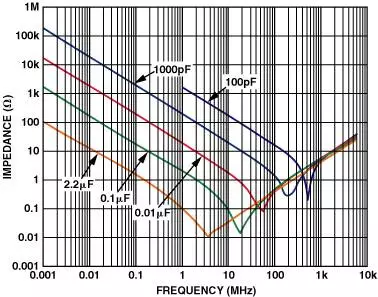
Figure1. Capacitance impedance versus frequency。
Start directly from the op amp's power supply pin;Capacitors with minimum capacitance and minimum physical size should be placed with op ampsPCBThe same side——And as close as possible to the amplifier。The ground terminal of the capacitor should be connected directly to the ground plane with the shortest pin or trace.。The above ground connection should be as close as possible to the load side of the amplifier to reduce interference between the power supply and ground.。Figure2This connection method is shown。
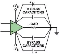
Figure2. Bypass power supply and ground shunt capacitor。
对于次大capacitance值的电容器应该重复这个过程。Best from0.01 ?FThe minimum capacitance value starts to be placed,And placed one close2.2 ?F(Or a little bigger)Low equivalent series resistance(ESR)Electrolytic capacitor。use0508Shell size0.01 ?FCapacitors have very low series inductance and excellent high frequency performance。
Power supply to power supply:Another configuration method uses one or more bypass capacitors across the positive and negative supply terminals of the op amp.。This method is usually used when it is difficult to configure four capacitors in the circuit.。Its disadvantage is that the size of the capacitor's outer casing may increase.,Because the voltage across the capacitor is twice the voltage in the single-supply bypass method。Increasing the voltage requires increasing the breakdown voltage of the device.,That is to increase the size of the outer casing。but,This method can be improvedPSRAnd distortion performance。
Because each circuit and wiring is different,So the configuration of the capacitor、The quantity and capacitance value must be determined according to the requirements of the actual circuit.。
Parasitic effect
The so-called parasitic effect is that those who slip into youPCBAnd destroying the circuit、a headache、Unexplained glitch(According to the literal meaning)。They are parasitic capacitances and parasitic inductances that are hidden in high-speed circuits.。These include parasitic inductances caused by package leads and traces that are too long.;Pad to ground、Parasitic capacitance formed between the pad to the power plane and between the pad and the trace;Interaction between through holes,And many other possible parasitic effects。Figure3(a)A typical in-phase operational amplifier schematic is shown。but,If parasitic effects are considered,The same circuit may become a graph3(b)That way。
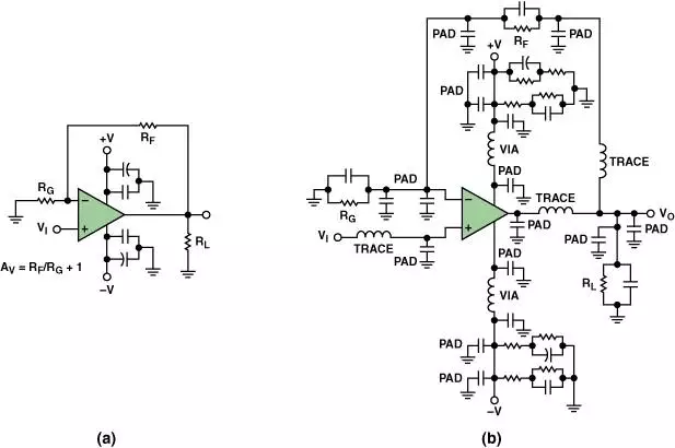
Figure3. Typical operational amplifier circuit,(a)Original design,(b)Figure after considering parasitic effects。
In high speed circuits,Small values can affect the performance of the circuit。Sometimes dozens of skins(pF)Capacitance is enough。Related examples:If only on the inverting input1 pFAdditional parasitic capacitance,It can cause almost in the frequency domain2 dBSharp pulse(See the figure4)。If the parasitic capacitance is large enough,It can cause instability and oscillation of the circuit。
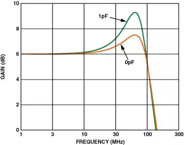
Figure4. Additional spikes caused by parasitic capacitance。
When looking for problematic parasitic sources,It may be possible to use several basic formulas for calculating the size of those parasitic capacitors mentioned above.。formula(1)Is to calculate parallel plate capacitors(See the figure5)Formula。
(1)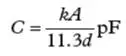
CRepresents the capacitance value,AExpresscm2Plate area,kExpressPCBRelative permittivity of materials,dExpresscmThe distance between the plates。
Figure5. Capacitance between two plates。
Strip inductors are another parasitic effect to consider,It is caused by the length of the printed line or the lack of a ground plane.。formula(2)Shows the calculation of the printed circuit inductance(Inductance)Formula。See picture6。 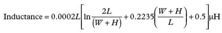
(2)
WIndicates the width of the printed line,LIndicates the length of the trace,HIndicates the thickness of the trace。All sizes aremmUnit。
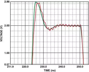
Figure6. Printed line inductance。
Figure7The oscillation in the middle shows the length of the non-inverting input of the high speed op amp2.54 cmInfluence of the printed line。Its equivalent parasitic inductance is29 nH(10-9H),Enough to cause sustained low pressure oscillation,Will last until the entire transient response cycle。Figure7Also shows how to use the ground plane to reduce the effects of parasitic inductance。
Figure7. Impulse response with and without ground plane。
Through hole is another parasitic source;They can cause parasitic inductance and parasitic capacitance。formula(3)Is a formula for calculating parasitic inductance(See picture8)。
(3)
TExpressPCBthickness of,dExpresscmThrough hole diameter。
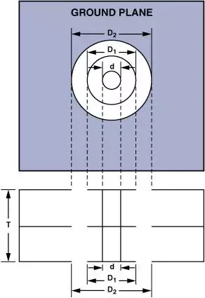
Figure8. Through hole size。
formula(4)Shows how to calculate through holes(See picture8)Parasitic capacitance value。
(4)
εrExpressPCBRelative permeability of the material。TExpressPCBthickness of。D1Indicates the diameter of the pad surrounding the via。D2Indicates the diameter of the isolation hole in the ground plane。All sizes arecmUnit。In one piece0.157 cmThickPCB上One通孔就可Take增加1.2 nHParasitic inductance and0.5 pFParasitic capacitance;That's why givingPCBAlways keep an alert when wiring,Minimize the effects of parasitic effects。
Ground plane
In fact, what needs to be discussed is much more than the ones mentioned in this article.,But we will highlight some key features and encourage readers to explore this topic further.。The relevant references are listed at the end of this article.。
The ground plane acts as a common reference voltage,Provide shielding,Ability to dissipate heat and reduce parasitic inductance(But it also increases the parasitic capacitance)Function。Although there are many benefits to using a ground plane,But you must be careful when implementing,Because it has some restrictions on what can and cannot be done.。
Ideally,PCBOne layer should be used exclusively as a ground plane。This will produce the best results when the entire plane is not destroyed.。Never use the area of the ground plane in this dedicated layer for other signals.。The ground plane can eliminate the magnetic field between the conductor and the ground plane,So you can reduce the inductance of the printed circuit。If destroying an area of the ground plane,Introduces unexpected parasitic inductance to the trace above or below the ground plane。
Because the ground plane usually has a large surface area and cross-sectional area,So keep the resistance of the ground plane to a minimum。In the low frequency band,Current will choose the path with the least resistance,But in the high frequency band,The current will select the path with the least impedance。
However there are exceptions,Sometimes a small ground plane will be better。If the ground plane is removed from the input or output pad,High speed op amps work better。Because of the parasitic capacitance introduced at the ground plane of the input,Increased input capacitance of the op amp,Reduced phase margin,Resulting in instability。As seen in the discussion of the Parasitic Effects section,Operational amplifier input1 pFCapacitance can cause very sharp spikes。Capacitive load at the output——Parasitic capacitive load——Causing the pole in the feedback loop。This will reduce the phase margin and cause the circuit to become unstable。
If possible,Analog and digital circuits——Including the respective ground and ground planes——Should be separated。A fast rising edge causes current spurs to flow into the ground plane。The noise caused by these fast current spurs can impair analog performance。Analog ground and digital ground(And power)Should be connected to a common ground point to reduce circulating digital and analog ground currents and noise。
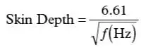
In the high frequency band,Must consider a kind of“Skin effect”The phenomenon。The skin effect causes the outer surface of the current flow guide——The result is a narrowing of the cross section of the wire,Therefore making DC(DC)Increased resistance。Although the skin effect is beyond the scope of this article,Here is still the skin depth in the copper wire(Skin Depth)a good approximation formula(以cmUnit):
(5)
Low sensitivity plating metal helps reduce skin effect。
Wiring and shielding
PCBThere are all kinds ofAnalog and digital signals,Including high to low voltage or current,FromDCToGHzFrequency Range。It is very difficult to ensure that these signals do not interfere with each other.。
Review the front“No one believes”Partial advice,The most important thing is to think ahead and how to deal with it.PCBSignal on the plan。It is important to note which signals are sensitive and determine what steps must be taken to ensure signal integrity.。The ground plane provides a common reference point for electrical signals,Can also be used for shielding。If signal isolation is required,First, you should leave a physical distance between the signal lines.。Here are some practical experiences worth learning from.:
Reduce the samePCBThe length of the medium long parallel line and the proximity of the signal printed line can reduce the inductive coupling。Reducing the length of long traces in adjacent layers prevents capacitive coupling。Signal lines that require high isolation should go through different layers and——If they are not completely isolated——Should take the orthogonal printing line,And place the ground plane between them。Orthogonal routing minimizes capacitive coupling,And the ground wire will form an electrical shield。This method can be used when constructing a control impedance trace。high frequency(RF)The signal usually flows on the control impedance trace。That is to say,The trace maintains a characteristic impedance,E.g50Ω(RFTypical value in the application)。Two of the most common control impedance traces,microstrip line4And stripline5Can achieve similar results,But the method of implementation is different。
Microstrip control impedance trace,As shown13Shown,Can be used inPCBArbitrary side;It directly uses the ground plane below it as its reference plane。
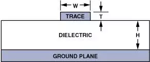
Figure13. Microstrip transmission line。
formula(6)Can be used to calculate a pieceFR4Characteristic impedance of the board。
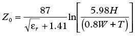
(6)
HIndicates the distance from the ground plane to the signal trace,WIndicates the width of the printed line,TExpress印制线厚度;All sizes are in mils(mils)(10-3inch)Unit。εr表示PCBDielectric constant of material。
Strip control impedance trace(See picture14)Two layers of ground plane,Signal printed circuit clipped in。This method uses more traces,needsPCBMore layers,Sensitive to changes in dielectric thickness,And the cost is higher——So usually only used in demanding applications。
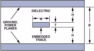
Figure14. Strip control impedance trace。
The characteristic impedance calculation formula for the strip line is as a formula(7)Shown。
(7)
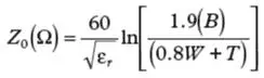
Protection ring,Or“Isolation ring”,Is another shielding method commonly used in operational amplifiers,It is used to prevent parasitic currents from entering sensitive nodes。The basic principle is very simple——Enclose the sensitive node completely with a protective wire,The wire remains or forces it to remain(Low impedance)The same potential as a sensitive node,So the absorbed parasitic current is far from the sensitive node。Figure15(a)Schematic diagram of a guard ring for op amp inverting and in-phase configuration is shown。Figure15(b)Shown forSOT-23-5Typical wiring method for two guard rings in a package。
Figure15. Protection ring。(a)Inverted and in phase operation。(b)SOT-23-5Package。
in conclusion
high levelPCBWiring is important for successful op amp circuit design,Especially for high speed circuits。A good schematic is the basis for good wiring;The close cooperation between circuit design engineers and wiring design engineers is fundamental,Especially about the location of the device and wiring。Issues to consider include bypass power,Reduce parasitic effects,Ground plane,Impact of op amp package,And wiring and shielding methods。
1.inPCBDesign time,Capacitors such as bypass filtering at the chip power supply should be as close as possible to the device,Typical distance is less than3MM。
2.The small ceramic bypass capacitor at the power supply of the op amp chip can provide the energy capacitance value for the high frequency characteristics of the amplifier when the amplifier is at the input high frequency signal. Depending on the frequency of the input signal and the speed of the amplifier, for example,一个400MHzAmplifier may be installed in parallel0.01uF和1nF电容。
3.When we buy devices such as capacitors,Also need to pay attention to his self-resonant frequency,Self-resonant frequency at this frequency(400MHz)Upper and lower capacitors have no benefit。
4.DrawingPCBTime,Do not walk the other lines below the input and output signal pins of the amplifier and the feedback resistor.,This can reduce the interaction of parasitic capacitance between different lines to make the amplifier more stable.
5.High-frequency new energy of surface mount devices is good and small
6.When wiring the board, keep the trace as short as possible while paying attention to his length and width to minimize parasitic effects.。
7.For the power line processing power line, the parasitic characteristics of the worst DC resistance and self-inductance, so we widen as much as possible when laying the power line
8.The current on the input and output cables of the amplifier is very small, so the parasitic effects they are very susceptible to are very harmful to them.
9.For more than1CMThe signal path is preferably terminated with controlled impedance and both ends(Matching resistor)Transmission line。
10.Amplifier drives a RC load. In order to solve the stability problem, a common technique is to introduce a resistor.ROUT Also close to the op amp This uses a series output resistor to isolate the capacitive load.。
Billion with core cityUnder the Shenzhen Xinjiasheng Industry and Trade Co., Ltd.,was founded in2013Year-on-line service,Main features of the mall platform“Online fast trade with a single+Offline entity supply delivery”The best of both worlds,It is a leading and professional e-commerce platform in China.+Physical store enterprise。Future developments and models are mainly(One-stop shop,Platform consignment/Handling idle inventory to achieve a win-win situation in resource sharing,Electronic Engineer Exchange Community,Interactive service platform such as hardware development and support)Providing accurate big data resource platform in this efficient and fast-growing technology Internet era。

 $1.805606/ 个
$4.583461/ 个
$44.445679/ 个
$1.875052/ 个
$0.611309/ 个
$11.389205/ 个
$0.555571/ 个
$1.805606/ 个
$4.583461/ 个
$44.445679/ 个
$1.875052/ 个
$0.611309/ 个
$11.389205/ 个
$0.555571/ 个


